Tensor G7 Codename "LaJolla" Explained: What the 2nm Chip Means for Pixel 12 Performance and AI
The smartphone industry is currently standing on the precipice of a massive hardware revolution, and Google is aggressively positioning itself at the absolute center of it. For years, the story of the Pixel lineup has been one of incredible software ambition crippled by inconsistent hardware execution. Buyers loved the cameras but loathed the battery life and thermal throttling. However, the Google Pixel 12 series leaks point to a monumental shift in 2027, driven entirely by a single piece of silicon.
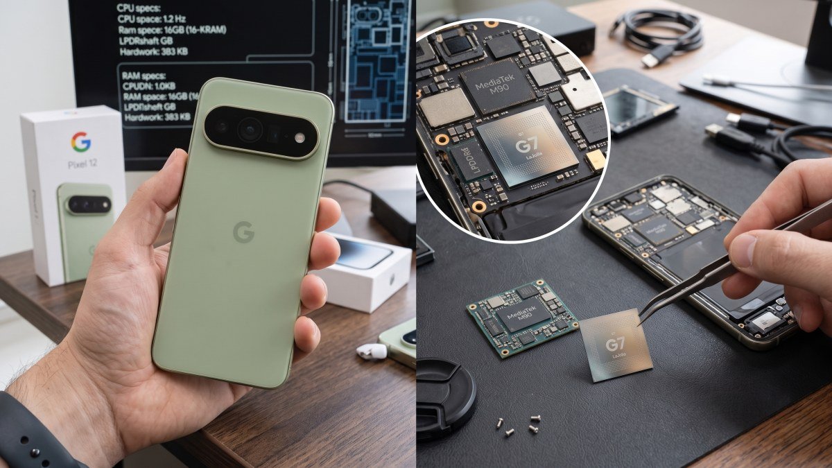
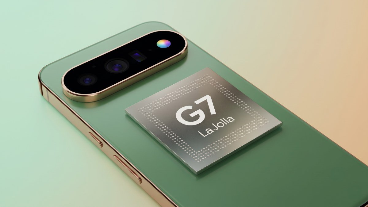
Internally at Google, this highly anticipated processor is operating under the codename "LaJolla". While the marketing department will eventually package this as the Tensor G7, understanding the LaJolla project is the key to understanding why the Pixel 12 is expected to be such a massive leap forward.
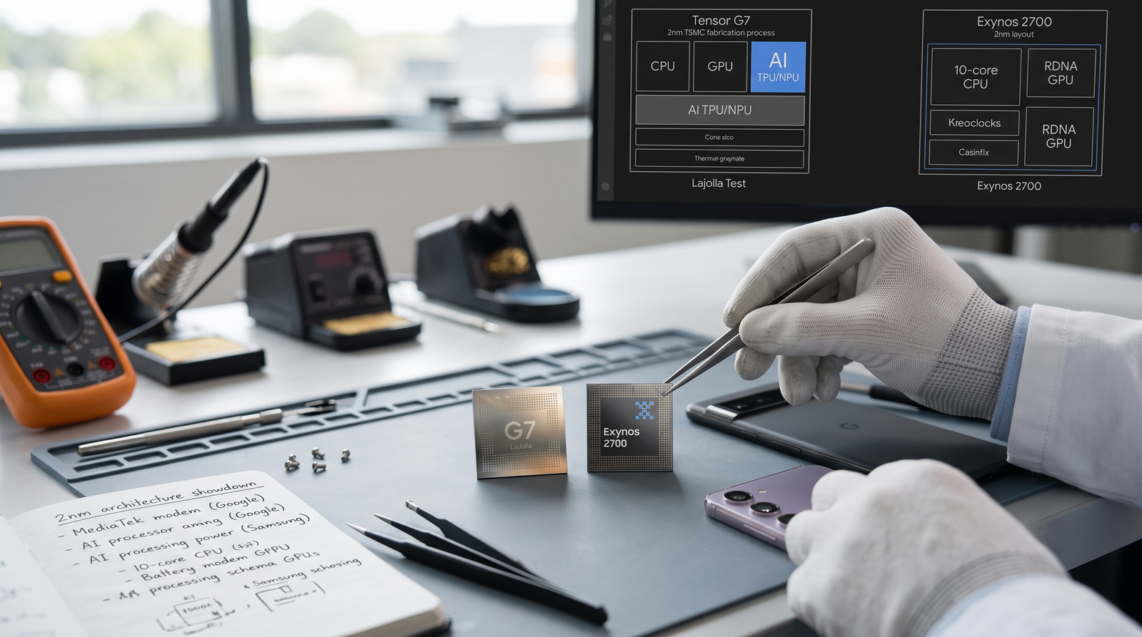
By completely severing its long-standing manufacturing ties with Samsung Foundry and embracing TSMC’s cutting-edge 2-nanometer (2nm) node, Google is rewriting the physical rulebook for its smartphones. Here is a deep dive into the LaJolla codename, the physics behind the 2nm manufacturing process, and what this radical hardware upgrade actually means for your daily battery life, gaming performance, and on-device artificial intelligence.
Decoding "LaJolla": A New Era for Google Silicon
Google’s hardware engineering teams have a long history of utilizing specific naming conventions for their internal projects. In the past, Tensor chips have often utilized codenames based on dog breeds or specific geographic locations. The choice of "LaJolla"—a wealthy, picturesque coastal neighborhood in San Diego, California—is highly symbolic within the tech industry.
San Diego is famously the global headquarters of Qualcomm, the undisputed king of Android processors. By adopting the LaJolla moniker, industry insiders believe Google is sending a very clear, confident signal: they are no longer just building "good enough" chips to run their camera software. The LaJolla project is an aggressive, direct challenge to Qualcomm's dominance.
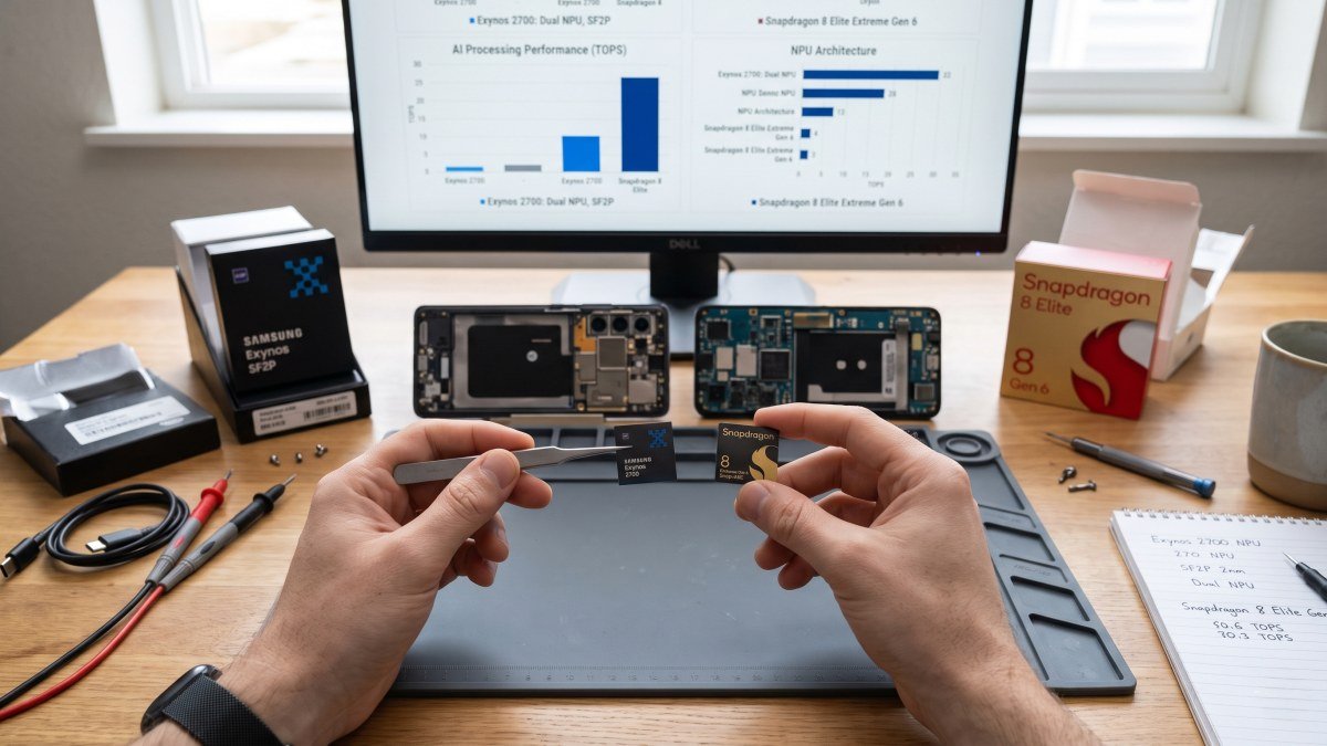
This codename represents the end of the "Samsung Era" for the Pixel lineup. From the original Tensor G1 through the Tensor G6, Google relied on Samsung's fabrication plants to build their chips. While this allowed Google to heavily customize the silicon, Samsung's manufacturing nodes consistently struggled with power efficiency and heat dissipation compared to their rivals. By shifting the LaJolla project entirely to Taiwan Semiconductor Manufacturing Company (TSMC), Google is finally putting its world-class chip design on the world's most efficient manufacturing foundation.
The Physics of TSMC's 2nm Node: Why It Matters
To truly grasp why the Pixel 12 TSMC 2nm upgrade is necessary, you have to understand the microscopic physics occurring inside the processor. A "nanometer" refers to the size of the transistors packed onto the silicon wafer. The smaller the transistor, the more you can fit into the exact same physical space.
Currently, premium flagship devices are built on 3nm or 4nm architectures. The Tensor G7 LaJolla chip makes the incredibly expensive leap to a 2nm node. At this microscopic scale, the transistors are packed so tightly together that the electrical signals have a significantly shorter distance to travel. This drastic reduction in travel distance fundamentally changes how the processor handles voltage.
Because the pathways are shorter, the chip requires significantly less raw electricity to push a signal from point A to point B. This translates directly to two massive real-world benefits for the Pixel 12:
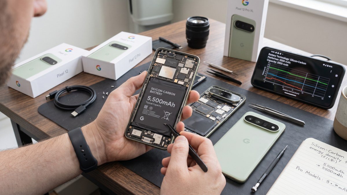
- Sustained Battery Endurance: By drawing less voltage for basic tasks like scrolling through social media or playing a YouTube video, the ambient battery drain drops significantly. This efficiency allows the Pixel 12 to easily push through a heavy workday without needing a mid-afternoon charge.
- Thermal Management: Less voltage equals less physical heat. Older Pixel phones were notorious for getting uncomfortably warm during long GPS navigation sessions or heavy mobile gaming. The 2nm LaJolla chip is designed to run incredibly cool, preventing the phone from thermally throttling its own performance just to stay safe.
Unlocking Persistent On-Device AI
The tech industry is currently obsessed with artificial intelligence, and Google is leading the charge with its Gemini Nano models. However, running complex AI algorithms requires an immense amount of continuous mathematical calculation. On older 4nm and 3nm processors, running a localized AI model in the background would rapidly drain the battery and cook the internal components.
The LaJolla project is explicitly engineered to solve this exact problem. By utilizing the ultra-efficient 2nm architecture, the Tensor G7 features a massive, dedicated Neural Processing Unit (NPU) that can remain active indefinitely without destroying the phone's battery life.
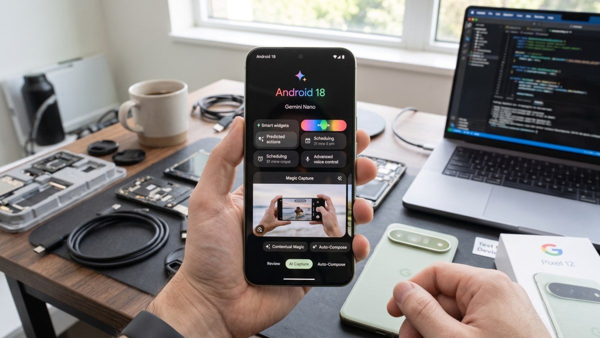
This allows the Pixel 12's Android 18 Gemini AI features to function seamlessly in the background. The phone will be able to constantly analyze your screen for context, predict your next action, summarize incoming notifications, and live-translate audio streams without ever sending your private data to a cloud server. The 2nm node provides the necessary thermal headroom to make "persistent AI" a reality, rather than just a battery-draining gimmick.
Gaming and Sustained Performance
When reviewing previous Google devices, such as the Pixel 11 Pro series, a common theme emerged: the phone could hit high benchmark numbers for the first five minutes of a heavy gaming session, but would inevitably slow down to prevent overheating. Gamers do not care about a five-minute peak; they care about sustained performance over a two-hour session.
The LaJolla chip aims to permanently fix this throttling issue. By pairing a custom Google-designed GPU with the TSMC 2nm node, the processor can maintain high graphical framerates indefinitely. Whether you are playing demanding titles like Genshin Impact or rendering 4K video timelines on the go, the Tensor G7 will hold its peak performance without aggressively dimming the screen or dropping frames to shed heat.
Furthermore, the LaJolla project includes a highly advanced memory controller designed to support LPDDR6 RAM. This next-generation memory standard provides an incredibly wide bandwidth, ensuring that the GPU and the NPU never have to wait for data to load, resulting in a buttery-smooth experience across the entire operating system.
The Ultimate Camera Brain: LaJolla's ISP
Finally, we cannot discuss a Pixel processor without analyzing its impact on photography. The Tensor G7 LaJolla includes a completely redesigned Image Signal Processor (ISP).
As we have previously detailed regarding the Pixel 12 camera upgrades and ISP features, moving the image processing to a 2nm node allows the phone to handle massive amounts of visual data instantly. The new ISP will enable hardware-level denoising in real-time, allowing you to capture Night Sight photos instantly without holding your hand perfectly still for several seconds.
More impressively, the LaJolla chip is expected to have the thermal capacity to run 8K Video Boost entirely on the device. Instead of uploading your videos to Google's servers for HDR enhancement, the Tensor G7 will process every single frame locally, delivering cinematic, professionally graded footage instantly to your camera roll.
Ultimately, the LaJolla codename represents the maturation of Google's hardware division. By finally combining their elite software engineering with the world's best 2nm manufacturing process, the Tensor G7 is poised to be the undisputed champion in the upcoming 2027 chip war. If you have been waiting for a Google phone that runs cool, lasts all day, and processes AI instantly, the LaJolla project is exactly what you have been holding out for.